Custom PCBs
All custom circuit boards were manufactured by our sponsor OSH Park PCBs, and our team assembled the components by hand. The CAD design was done in KiCAD, and all designs are public on our team’s GitHub organization.
Power Distribution Board (PDB)
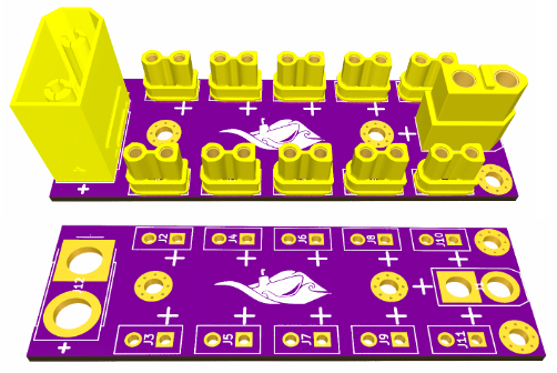
The power distribution board is made of extra 2 oz copper to handle high current, and consists of several PCB-mount XT connectors of varying size. These boards provide an excellent and neat way to distribute power, as compared to a traditional bus bar. The genders of the XT-60 and -90 connectors can be easily changed to fit the required configuration, as we do in the Compute hull. While the Actuator hull’s PDB runs at unregulated 5S battery voltage (16V-21V), the Compute hull’s PDB is spliced off of a buck converter, and powers its components with regulated 12V power.
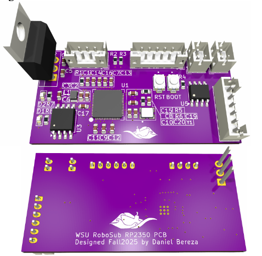
RP2350 Mainboard (V2)
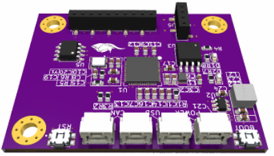
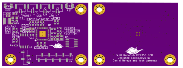
The main powerhouse of our team’s custom PCBs is a mainboard developed around the RP2350 microcontroller. Packaged with flash memory, a CAN controller, and many GPIO and PWM output ports, the board is designed to serve as a sort of “base” board for additional daughterboards or “hats” to stack on top of.
The board features a reset and boot pushbutton, as well as power, CAN in, CAN out, and USB debugging locking JST ports. The two SMD socket headers are for stacking additional boards on top and expose power and IO to the daughterboard. The buttons and JST plugs face sideways, to allow access even when a board is stacked. To access the USB interface, team members can plug a small USB-C adapter board to the USB and POWER plugs. The board also has two red LEDs: one that indicates power, and another that shows activity via a GPIO pin.
We chose to use the RP2350 microprocessor rather than an STM or ESP based one for several reasons. First, STM processors are notoriously difficult to program and manage, and we liked the configurability and reputation offered by the RP2350 controller. We determined that ESP boards would be overkill for our use case, given that they have WiFi and Bluetooth capabilities. Finally, the PIO capabilities of the RP chip coupled with unparalleled PWM channels made the RP2350 chip a clear choice.
As with all of our custom PCBs, the mounting holes are spaced on a 10mm grid pattern to accommodate our electrical shelving.
PWM Daughterboard
The PWM daughterboard is currently our only daughterboard designed for the RP board, although several more are in the works for next season. The daughterboard simply exposes 10 PWM channels as ground/signal pairs via locking JST GH connectors. We use one of these in our Actuator hull to drive the 8 BLHeli_S ESCs for the T200 thrusters, as well as the disable/enable reed switch and the tube’s LEDs.
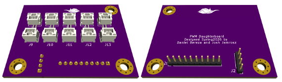
The board neatly stacks on the base board, allowing a compact layout and decreasing the number of wires. The board also acts as a ground bus, letting each JST connector share a common ground without the need for a separate ground splice to each motor controller.
Version 1: Original RP2350 Development Mainboard
Before its current “V2” designation, we manufactured an additional development board of the RP2350 PCB, the “V1.” Renderings are shown here for posterity. While the overall design stayed the same, we changed the layout to accommodate daughterboards, added mounting holes, and decreased the regulator size.
Anti-Spark Switch Control ESP
Our FlipSky anti-spark relay switch, which controls the main power input to the submarine, comes with a momentary button switch. While this is great for skateboards and bikes, we prefer the Blue Robotics rotary switches. We use a small ESP powered off a buck converter directly from the battery to read the state of the external switch and act as a proxy to send signal pulses to the main anti-spark switch. While this is not a custom PCB, we have plans to make it one in the future and extend our power capabilities. For more details on how this works, see Appendix G for additional schematics.